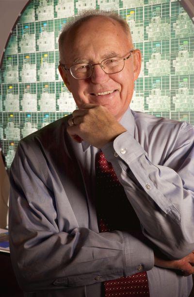
A 2005 photograph of Gordon E Moore
While chips have become ubiquitous, Moore’s Law has remained a self-fulfilling prophecy even half a century later. Not bad for an industry where the time scale is not measured in decades and centuries, but in annual quarters, says Shivanand Kanavi.
‘The complexity [of integrated circuits] for minimum costs has increased at a rate of roughly a factor of two per year. -- Gordon E Moore, Electronics, VOL 38, NO 8, 1965
This year marks 50 years of the reign of Moore's Law. Gordon Moore, the co-founder of Intel, made a prediction in 1965 that the number of transistors on a chip and the raw computing power of microchips would double every year while the cost of production would remain the same.
When he made this prediction, chips had only 50 transistors; today, a chip can have more than four billion transistors. Thus, the power of the chip has increased by a factor of 80 million in about 38 years!
The only correction to Moore’s Law is that nowadays the doubling occurs every 18 months, instead of a year. As for cost, when transistors were commercialised in the early 1950s, one of them used to be sold for $49.95; in 2015 a chip like the 18 Core Xeon Haswel EP, which has 5.5 billion transistors, costs about $4,000. In other words, the cost per transistor has dropped by a factor of 70 million.
 This is what has made chips affordable for all kinds of applications: Personal computers that can do millions of arithmetic sums in a second, telecom networks that carry billions of calls, and Internet routers that serve up terabytes of data (a tera byte is a thousand billion byte).
The reduced costs allow chips to be used in a wide range of modern products. They control cars, microwave ovens, washing machines, cell phones, television sets, machine tools, wrist-watches, radios, audio systems and even toys.
In the not too distant future, the Government of India may consider the idea of providing a billion Indians with a chip-embedded Aadhar card carrying all personal data needed for public purposes. Already credit cards, debit cards, driving licences etc in India carry chips.
According to the US Semiconductor Industry Association, the industry produces a billion transistors per year for every person on earth (seven billion inhabitants)! The global semiconductor industry is estimated to be a $300 billion-a-year business. Electronics, a technology that was born at the beginning of the 20th century with the discovery of the electron, has today been integrated into everything imaginable.
 The Nobel Committee paid the highest tribute to this phenomenal innovation in 2000 when it awarded the Nobel Prize in Physics to Jack Kilby who invented the integrated circuit, or the chip, at Texas Instruments in 1958. Considering the breathtaking advances in the power of chips and the equally astonishing reduction in their cost, people sometimes wonder whether this trend will continue forever. Or will the growth come to an end soon and the so-called Moore's Law cease to be valid?
The Institute of Electrical and Electronics Engineers, or (IEEE as ‘I-triple E’) -- the world’s most prestigious and largest professional association of electrical, electronics and computer engineers -- conducted a survey among 565 of its distinguished fellows, all highly respected technologists.
One of the questions the experts were asked was: How long will the semiconductor industry see exponential growth, or follow Moore’s Law? The results of the survey, published in the January 2003 issue of IEEE Spectrum magazine, saw the respondents deeply divided.
An optimistic 17 per cent said more than 10 years, a majority-- 52 per cent -- said five to 10 years and a pessimistic 30 per cent said less than five years. More than 10 years after the survey, the law still seems to be going strong.
Printing technology and chip-making
The chip-making process, in its essence, resembles the screen-printing process used in the textile industry. When you have a complicated, multi-coloured design to be printed on a fabric, the screen printer takes a picture of the original, transfers it to different silk screens by a photographic process, and then uses each screen as a stencil, while the dye is rolled over the screen. One screen is used for each colour. The only difference is in the size of the design.
 With dress material, print sizes run into square metres; with chips, containing millions of transistors (the 6 core i7, for example, has 1.2 billion transistors), each transistor occupies barely a square micron.
How is such miniature design achieved?
There are all kinds of superfine works of art, including calligraphy of a few words on a grain of rice. But the same grain of rice can accommodate a complicated circuit containing about 3,000 transistors!
How do chipmakers pull off something so incredible?
In a way, the chip etcher’s approach is not too different from that of the calligraphist writing on a grain of rice. While the super-skilled calligraphist uses an ordinary watchmaker’s eyepiece as a magnifying glass, the chipmaker uses very short wavelength light (ultraviolet light) and sophisticated optics to reduce the detailed circuit diagrams to a thousandth of their size.
These films are used to create stencils (masks) made of materials that are opaque to light. The masks are then used to cast shadows on photosensitive coatings on the silicon wafer, using further miniaturisation with the help of laser light, electron beams and ultra-sophisticated optics to imprint the circuit pattern on the wafer.
The process is similar to the good old printing technology called lithography, where the negative image of a text or graphic is transferred to a plate covered with photosensitive material, which is then coated by ink that is transferred to paper pressed against the plates by rollers. This explains why the process of printing a circuit on silicon is called photolithography.
Of course, we are greatly simplifying the chip-making methodology for the sake of explaining the main ideas. In actual fact, several layers of materials -- semiconductors and metals -- have to be overlaid on each other, with appropriate insulation separating them.
Chipmakers use several sets of masks, just as newspaper or textile printers use different screens to imprint different colours in varied patterns. While ordinary printing transfers flat images on paper or fabric, chipmakers create three dimensional structures of micro hills and vales by using a host of chemicals for etching the surface of the silicon wafer.The fineness of this process is measured by how thin a channel you can etch on silicon. So, when someone tells you about 45 nanometre (nanometre is one millionth of a milli metre) technology being used by leading chipmakers, they are referring to hi-tech scalpels that can etch channels as thin as 45 nanometres. To get a sense of proportion, that is equivalent to etching over 2,000 parallel ridges and vales on the diameter of a single strand of human hair!
In 2010 most fabs used 45 nanometre technology; in 2015 many leading fabs have commercialised 22 nanometre technology and are experimenting with 14 nanometre technology in their labs.
Read more.......
.png)

 This is what has made chips affordable for all kinds of applications: Personal computers that can do millions of arithmetic sums in a second, telecom networks that carry billions of calls, and Internet routers that serve up terabytes of data (a tera byte is a thousand billion byte).
 The Nobel Committee paid the highest tribute to this phenomenal innovation in 2000 when it awarded the Nobel Prize in Physics to Jack Kilby who invented the integrated circuit, or the chip, at Texas Instruments in 1958. Considering the breathtaking advances in the power of chips and the equally astonishing reduction in their cost, people sometimes wonder whether this trend will continue forever. Or will the growth come to an end soon and the so-called Moore's Law cease to be valid?
 With dress material, print sizes run into square metres; with chips, containing millions of transistors (the 6 core i7, for example, has 1.2 billion transistors), each transistor occupies barely a square micron.

0 comments: